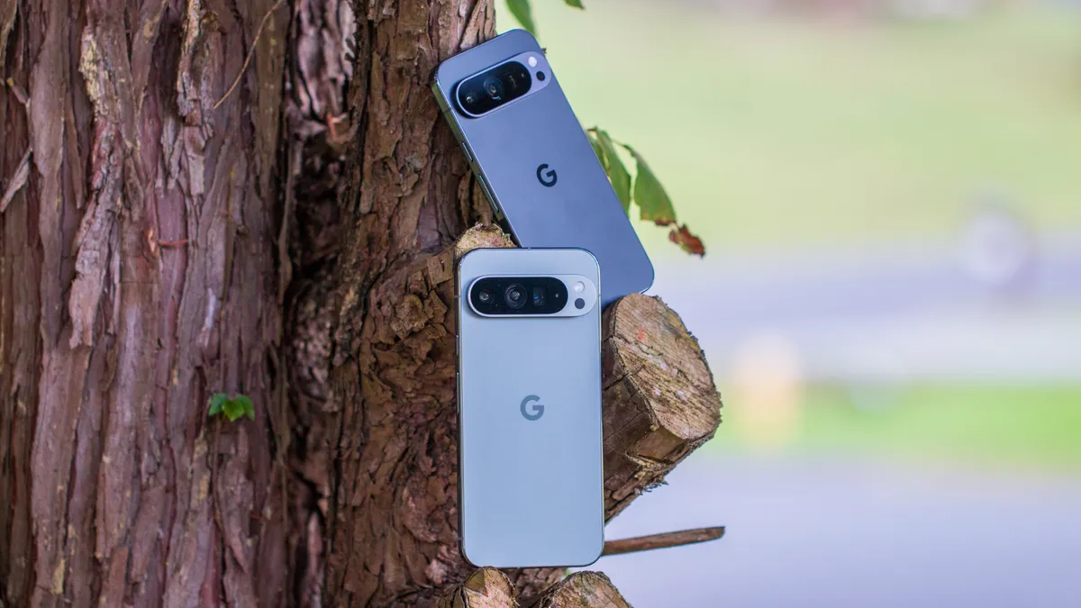
Google has equipped Pixel smartphones with its own in-house systems-on-a-chip (SoCs) for four generations. While the company designs the majority of Tensor processors, it doesn’t make them; instead, it chooses to outsource the fabrication of these chips to Samsung Foundry. This year that may change, as the unannounced Tensor G5 SoC will reportedly be produced by Taiwan Semiconductor Manufacturing Company (TSMC).
TSMC is far and away the industry leader in semiconductor manufacturing, and the best smartphone processors — including the Apple A18 Pro and the Qualcomm Snapdragon 8 Elite — use its flagship 3nm process node. Google will reportedly begin using TSMC’s 3nm process to make its Tensor G5 processors, opening the door for big performance and quality improvements. But how big of a deal is it really to the average user?
This week, Android Authority revealed a detailed component list for the Tensor G5 SoC, shedding light on the planned changes. According to the report, these are the supposed changes Google will make to Tensor chips, starting with the Tensor G5:
|
Component |
Tensor G1-G4 |
Tensor G5 |
|---|---|---|
|
CPU |
Arm Cortex |
Arm Cortex |
|
GPU |
Arm Mali |
Imagination Technologies DXT |
|
Audio processor |
Google AoC |
Google AoC |
|
Memory compressor |
Google Emerald Hill |
Google Emerald Hill |
|
DSP |
Google GXP |
Google GXP (next-generation) |
|
TPU |
Google EdgeTPU |
Google EdgeTPU (next-generaiton) |
|
Video codec |
Google BigWave (AV1); Samsung MFC (other formats) |
Chips&Media WAVE677DV |
|
Display controller |
Samsung DPU |
VeriSilicon DC9000 |
|
Image-signal procesor |
Samsung ISP with custom Google blocks |
Google ISP |
|
MIPI DSI PHY, CSI PHY, DisplayPort PHY, I3C, I2C, SPI, LPDDR5x PHY |
Samsung |
Synopsys DesignWare IP cores |
|
SPMI controller |
Samsung |
SmartDV SPMI |
|
PWM controller |
Samsung |
Faraday Technologies FTPWMTMR010 |
|
UFS controller |
Samsung |
Unknown |
|
USB3 core |
Synopsys DesignWare USB3 |
Synopsys DesignWare USB3 |
A switch from Samsung Foundry to TSMC should result in a few high-level benefits for Google. For starters, Samsung Foundry has struggled to make smaller chips reliably at desirable yield rates. Its issues designing 4nm and smaller chips have been well-documented, and it’s reported that unfavorable yield rates are the reason there isn’t an Exynos-powered Samsung Galaxy S25 model.
Meanwhile, TSMC’s advanced processors have been around longer, and its manufacturing processes are likely more reliable than those of Samsung Foundry. For instance, overheating was a key problem for Apple’s A17 Pro chip, which was manufactured using TSMC’s older 3nm process. It already worked out those kinks, and Google can reap the benefits with the Tensor G5.
As our own Jerry Hildenbrand recently unpacked, 3nm processors can fit more components or run more efficiently than larger SoCs. However, it’s often the other kinds of engineering work that make a tangible difference. That’s why Google’s component swaps rumored for the Tensor G5 could make all the difference.
What may change with the Tensor G5
Samsung-fabricated Tensor processors often use off-the-shelf components manufactured by the South Korean company to fill in the gaps between Google’s custom designs. With the TSMC-fabricated Tensor G5, Google is taking the opportunity to design more of its own components.
The most eye-catching part of the leaked spec sheet is certainly the Google-design image-signal processor (ISP) set to become part of the Tensor G5 chip.
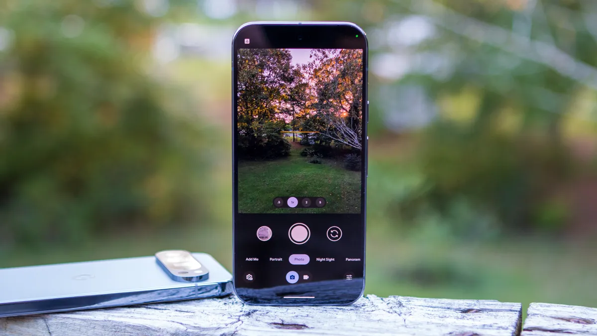
ISPs are responsible for processing the information coming in from a phone’s camera lenses, and they are crucial to getting great-quality photos and videos. A bad ISP can cause excellent camera lenses to produce poor output and vice versa. As such, we might be able to expect better photos and videos from the same camera hardware with the Tensor G5 chip and beyond.
Older Pixel phones, like the Tensor G4-powered Pixel 9, used Samsung-designed ISPs with small Google tweaks. Now that Google is purportedly developing a custom ISP from start to finish, it’s likely that future Pixel flagships will have hardware and software stacks that are better optimized, at least where the cameras are concerned.
Additionally, Google is reportedly replacing Samsung-made controllers — like the USB and display controllers — with licensed parts from companies such as Synaptics. This could give the company more or less flexibility in tweaking and optimizing how they work with Pixel hardware, depending on how they are implemented.
What wouldn’t change with the Tensor G5

The reason why you might think a switch to TSMC isn’t a big deal is that there are a few major holdovers from the Samsung Foundry era. While the GPU included in the Tensor G5 is predicted to be the Imagination Technologies DXT, the CPU will still feature Arm Cortex cores. Aside from the bump that comes with moving from a 4nm to a 3nm process, that means the Tensor G5 could perform similarly to older generations.
The Tensor G5’s audio processor, memory controller, digital signal processor, and tensor processing unit will all still be custom components designed by Google. The latter two components are tabbed to be next-generation versions specifically for the Tensor G5. As the TPU handles AI-based tasks, this could be a sign that the Tensor G5 in the Google Pixel 10 may be able to handle more AI operations on-device.
With all these holdovers, plus the same USB3 controller, it’s not like Google is completely starting over with the Tensor G5 chip.
A TSMC-made Google Tensor chip opens new possibilities

I’m optimistic that the switch from Samsung Foundry to TSMC could give Google more flexibility in designing future Tensor chips, including the Tensor G5, that are better optimized for Pixel phones. While it’s true that Google would likely still use off-the-shelf components for some parts of the SoC, it would have more flexibility in choosing which components are best fit for Pixel hardware needs. Previously, Tensor chips seemed to default to Samsung components when a third-party option was needed.
For example, the pulse-width modulation (PWM) controller in the Tensor G5 is said to be the Faraday Technologies FTPWMTMR010. Those who aren’t PWM-sensitive might not notice such a small tweak, but Pixel phones are known for having extremely low PWM frequencies. These can cause pain and headaches for a portion of the population, and the switch from a Samsung controller to a Faraday Technologies controller could give Google the flexibility to natively offer higher PWM rates — or disable PWM altogether.
It’s unclear whether Google would do something like this, but that’s the dream scenario for a move such as this one. Ideally, the switch from Samsung Foundry to TSMC could give Google the flexibility to identify problems with its hardware and correct them, either with off-the-shelf parts or custom components. If Google can take these kinds of steps, we’ll look back on the Tensor G5 switch as a turning point for Pixel hardware.